Fermi Level In Semiconductor : Fermi Energy Level For Ptype Extrinsic Semiconductors Class 12 Physics Cbse - Energy level of conduction band consists of the electrons which are responsible for conduction.
bymagasoberanes-
0
Fermi Level In Semiconductor : Fermi Energy Level For Ptype Extrinsic Semiconductors Class 12 Physics Cbse - Energy level of conduction band consists of the electrons which are responsible for conduction.. In a perfect semiconductor (in the absence of impurities/dopants), the fermi level lies close to the middle of the band gap 1. Of holes in valance band are not equal. In fact, this level is called the intrinsic fermi level and shown by e i: The density of electrons in the conduction band equals the density of holes in the valence band. If you can bring the fermi level high enough, then part of the tail will go over to the conduction band.
Where the fermi energy is located (correct?). I can understand that the distribution changes with the temperatures (it gets broader) but i don't understand why/how the fermi level changes. Position of fermi level in intrinsic semiconductor | semiconductors ||jntuk| r20 | 2021|mixed telugu| Green, unsw) illustrating the location of the fermi level e f relative to the valence and conduction bands for various materials. However as the temperature increases free electrons and holes gets generated.
Gate Ese Detailed Explanation For Fermi Energy Level In N Type Semiconductor In Hindi Offered By Unacademy from edge.uacdn.net Due to lack of sufficient energy at 0 kelvin, the fermi level can be considered as the sea of fermions (or electrons) above which no electrons exist. At absolute zero temperature intrinsic semiconductor acts as perfect insulator. The electrical conductivity of the semiconductor depends upon. Above is a diagram (ref. 1.1 0, indicating equal concentrations of electrons and holes. The fermi level is the energy separating occupied states of the valence band from empty states of the conduction band at the absolute temperature t=0 kelvin. For the intrinsic semiconductor at 0k, However as the temperature increases free electrons and holes gets generated.
Fermi levelis the state for which there is a 50% probability of occupation.
The density of electrons in the conduction band equals the density of holes in the valence band. In a perfect semiconductor (in the absence of impurities/dopants), the fermi level lies close to the middle of the band gap 1. Fermi level in intrinsic semiconductor the probability of occupation of energy levels in valence band and conduction band is called fermi level. Fermi level lies in the midway between the valence band top and conduction band bottom of an intrinsic semiconductor, as shown in fig. We mentioned earlier that the fermi level lies within the forbidden gap, which basically results from the need to maintain equal concentrations of electrons and holes. Due to lack of sufficient energy at 0 kelvin, the fermi level can be considered as the sea of fermions (or electrons) above which no electrons exist. The fermi level lies between the valence band and conduction band because at absolute zero temperature the electrons are all in the lowest energy state. The fermi level is the surface of fermi sea at absolute zero where no electrons will have enough energy to rise above the surface. 1.1 0, indicating equal concentrations of electrons and holes. Fermi energyis the difference highest occupied state and lowest occupied state at 0k. For si withnd= 1015 cm3andni = 1010 cm3, using equation 3, ef nis 0.25evaboveef i. Fig.2.7.2 graphical solution of the fermi energy based on the general analysis. Of holes in valance band are not equal.
Green, unsw) illustrating the location of the fermi level e f relative to the valence and conduction bands for various materials. Fermi level is the highest energy level occupied by the electrons in the material at absolute zero temperature. Fermi level in extrinsic semiconductor 1. Above is a diagram (ref. Fermi energyis the difference highest occupied state and lowest occupied state at 0k.
Fermi Level In Extrinsic Semiconductor from image.slidesharecdn.com I can understand that the distribution changes with the temperatures (it gets broader) but i don't understand why/how the fermi level changes. Due to lack of sufficient energy at 0 kelvin, the fermi level can be considered as the sea of fermions (or electrons) above which no electrons exist. The fermi level is the level where the probability that an electron occupies the state is 0.5, e.g. The term fermi level is mainly used in discussing the solid state physics of electrons in semiconductors, and a precise usage of this term is necessary to describe band diagrams in devices comprising different materials with different levels of doping. Fermi level is a kind of measure of equilibrium electronic energy of a solid material. Fig.2.7.2 graphical solution of the fermi energy based on the general analysis. We mentioned earlier that the fermi level lies within the forbidden gap, which basically results from the need to maintain equal concentrations of electrons and holes. By small thermal energy or by applying electric field, this electron can be easily excited from the valence band to the conduction band.
Semiconductor doping and higher temperatures can greatly improve the conductivity of the pure semiconductor material.
The electrical conductivity of the semiconductor depends upon. Fig.2.7.2 graphical solution of the fermi energy based on the general analysis. The fermi level is the energy separating occupied states of the valence band from empty states of the conduction band at the absolute temperature t=0 kelvin. I can understand that the distribution changes with the temperatures (it gets broader) but i don't understand why/how the fermi level changes. For the intrinsic semiconductor at 0k, The fermi level is the surface of fermi sea at absolute zero where no electrons will have enough energy to rise above the surface. Where the fermi energy is located (correct?). The fermi level is the level where the probability that an electron occupies the state is 0.5, e.g. Fermi level of metal and semiconductors: The fermi level is referred to as the electron chemical potential in other contexts. Fermi level of intrinsic semiconductor those semi conductors in which impurities are not present are known as intrinsic semiconductors. The term fermi level is mainly used in discussing the solid state physics of electrons in semiconductors, and a precise usage of this term is necessary to describe band diagrams in devices comprising different materials with different levels of doping. Kb is the boltzmann constant.
Fermi level of metal and semiconductors: Semiconductor doping and higher temperatures can greatly improve the conductivity of the pure semiconductor material. In a perfect semiconductor (in the absence of impurities/dopants), the fermi level lies close to the middle of the band gap 1. The value for the fermi energy and carrier density is obtained at the crossing (indicated by the arrow) of the two black curves which represent the total positive and total negative charge in the semiconductor. Of electrons in conduction band and no.
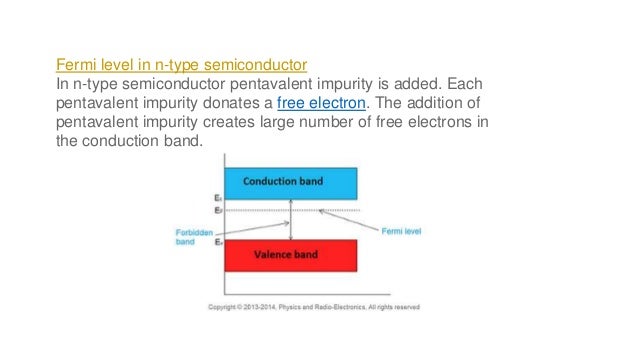
Fermi Edge The Xps Library Of Monochromatic Xps Spectra from i2.wp.com Whenever the system is at the fermi level, the population n is equal to 1/2. Kb is the boltzmann constant. The term fermi level is mainly used in discussing the solid state physics of electrons in semiconductors, and a precise usage of this term is necessary to describe band diagrams in devices comprising different materials with different levels of doping. If you can bring the fermi level high enough, then part of the tail will go over to the conduction band. Fermi level in extrinsic semiconductor fermi level in extrinsic semiconductor in extrinsic semiconductor, the number of electrons in the conduction band and the number of holes in the valence band are not equal. Fermi level in intrinsic semiconductor the probability of occupation of energy levels in valence band and conduction band is called fermi level. Of holes in valance band are not equal. Fermi level lies in the midway between the valence band top and conduction band bottom of an intrinsic semiconductor, as shown in fig.
At absolute zero temperature intrinsic semiconductor acts as perfect insulator.
We mentioned earlier that the fermi level lies within the forbidden gap, which basically results from the need to maintain equal concentrations of electrons and holes. The density of electrons in the conduction band equals the density of holes in the valence band. This definition of fermi energy is valid only for the system in which electrons are free (metals or superconductor), or any system. (a) fermi level position in pure semiconductors at this point, we should comment further on the position of the fermi level relative to the energy bands of the semiconductor. In electrical insulators and semiconductors, the valence band is the highest range of electron energies in which electrons are normally present at. Fermi levelis the state for which there is a 50% probability of occupation. These electrons jumps up from the valence shell and becomes free. The fermi energy is defined as: Fermi energyis the difference highest occupied state and lowest occupied state at 0k. The value for the fermi energy and carrier density is obtained at the crossing (indicated by the arrow) of the two black curves which represent the total positive and total negative charge in the semiconductor. Position of fermi level in intrinsic semiconductor | semiconductors ||jntuk| r20 | 2021|mixed telugu| Fermi level in extrinsic semiconductor fermi level in extrinsic semiconductor in extrinsic semiconductor, the number of electrons in the conduction band and the number of holes in the valence band are not equal. The fermi level is referred to as the electron chemical potential in other contexts.